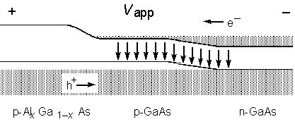
Triple layer structure: a p-type AlxGa1-xAs layer next to a p-type GaAs layer, followed by an n-type GaAs layer.The AlxGa1-xAs layer has a larger band gap energy than the GaAs layer.The presence of the larger band gap layer forces the electrons to stay within the GaAs region.Under high forward bias in an appropriately shaped cavity, there are a large number of holes in the valence band that combine with a large number of electrons, yielding lasing.
|